Bit-Slice Design: Controllers and ALUs
by Donnamaie E. White
Copyright © 1996, 2001, 2002 Donnamaie E. White
- Pre-Introduction
- Selection of the Implementation
- Microprogramming
- Advantages of LSI
- The 2900 Family
- Language Interrelationships
- Controller Design
- Constructing the CCU
- Sequential Execution
- Multiple Sequences
- Start Addresses
- Mapping PROM
- Unconditional Branch
- Conditional Branch
- Timing Considerations
- Pipelining
- Improved Architecture
3. Adding Programming
Support to the Controller
- Expanded Testing
- Subroutines
- Nested Subroutines
- Stack Size
- Loops
- Am29811
- Am2909/11
- CASE Statement (Am29803A)
- Microprogram Memory
- Status Polling
- Interrupt Servicing
- Implementation - Interrupt Request Signals
- Vector Mapping PROM
- Next Address Control
- Am2910
- Am2910 Instructions
- Control Lines
- Interrupt Handling
- Am2914
- Interconnection of the Am2914
6. The ALU and Basic Arithmetic
- Further Enhancements
- Instruction Fields
- Instruction Set Extensions
- Sample Operations
- Arithmetic -- General
- Multiplication with the Am2901
- Am2903 Multiply
Adding Programming Support to the ControllerLast Edit September 24, 1996; May 1, 1999; July 7, 2001 Microprogram MemoryThe microprogram memory is implemented in ROMs when a final design is debugged and a high volume production run is anticipated. ROMs carry a mask charge for their factory programming, and the production volume must be sufficient to absorb this charge. Low volume production and prototypes are implemented in PROMs, erasable PROMs (EEPROMS), or writable control stores. In the PROM family, registered PROMs, memories with on-board pipeline registers, also exist. [Early 1980s] AMD's Am27S27The Am27S27 was a registered PROM. It was organized as a 512 by 8 array, with nine (9) address lines and two (2) enable lines. The worst-case time between the address being presented and the data being ready to enter the register was 50ns and referred to as the address to Cp(high) to set-up time, ts(A). The register must be output-enabled, E'1 and E'2 both LOW, and clocked to load the data. Data are available at the output in 20ns (worst-case) referred to as the delay from Cp(high) to output, tPHL(Cp), tPLH(Cp), assuming that the chip is already enabled. (Refer to the Am27S27 data sheet if you can find one.) If the chip is not enabled, the time delay is 25ns worst-case. Only the portion of the microword containing the branch address need be under output control. The remaining output enables may be used to allow large PROM memories to be constructed. Most 1K - 4K words deep. Sample DesignAssume that a 512 by 80 memory is desired. Using the Am27S27 (tristate), ten chips must be placed in parallel with all address and enable lines common (Figure 3-10). Figure 3-10 512 by 80 Am27527 memory, initial layout.
The first item that needs to be investigated is DC loading. Assume that the memory is connected to three Am2911 microprogram sequencers, which provide the required 9-bit address (2**n = 512). Each address line carries ten times the loading represented by one Am27S27. From the data sheets, we get the information in Table 3-3. The Am2911 can drive 48 loads. The 512 x 80 memory presents 10 loads; thus there is no problem here.
What about AC loading? The Am27S27 will present a capacitive load of 10 x 5pF = 50pF, which, in the Am2911 specification, is the number for which the Am2911 timing is characterized; therefore, there will be no degradation of Am2911 performance.
Table 3-3 Data on DC Loading
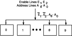
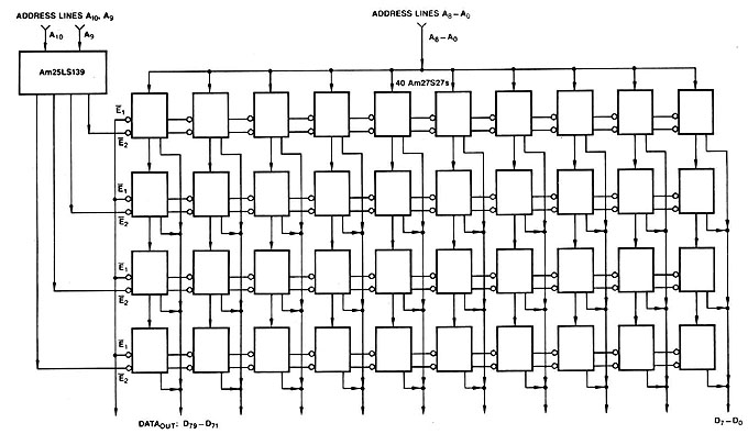
Sample Design 2Assume that a 2K x 80 memory is desired. This requires that an Am25LS139 Decoder (or comparable device) be used to decode the two added high-order address bits into output enable E'2 signals. Three Am2911 units are required to supply the 11-bit address. The configuration is shown in Figure 3-11, which details the basic interconnections. Figure 3-11 2K by 80 Am27527 memory. Only one "row" of 27527s are enabled at any one time.
The address lines are loaded with 4 x 10 = 40 loads, under the 48 load limit; therefore, no buffer drivers are required. The Am27S27S devices are switched by row and are not always enabled. When the enable signal is switched, there is an added delay of 5ns using tPZL(CP), tPZH(CP) as the device switches from its high-impedance state to active output, making the total delay from clock to output 25ns worst case. The AC loading is significant with 40 x 5pF = 200pF loading on each Am2911 address line. The Am2911 performance must be degraded in accordance with this increased capacitive load by 0.1ns per pF over 50pF: 200pF - 50pF = 150pF 0.1ns/pF x 150pF = 15ns added delay to the Am2911 propagation time There is no way to avoid the delay. Any buffer drivers inserted between the Am2911 and the Am27S27 array, while removing the Am2911 degradation, would add a propagation delay of their own of an approximately equivalent magnitude. The 0.1ns/pF degradation figure is conservative, and measurements have shown that the actual degradation is somewhat less (0.07ns/pF), but it is the accepted figure for worst-case timing, where conservative estimates are desirable. |