Chapter start Previous page Next page
2.6.3 A Simple Example
How do we make and use datapath elements? What does a design look like? We may use predesigned cells from a library or build the elements ourselves from logic cells using a schematic or a design language. Table 2.12 shows an 8-bit conditional-sum adder intended for an FPGA. This Verilog implementation uses the same structure as Figure 2.25, but the equations are collapsed to use four or five variables. A basic logic cell in certain Xilinx FPGAs, for example, can implement two equations of the same four variables or one equation with five variables. The equations shown in Table 2.12 requires three levels of FPGA logic cells (so, for example, if each FPGA logic cell has a 5 ns delay, the 8-bit conditional-sum adder delay is 15 ns).
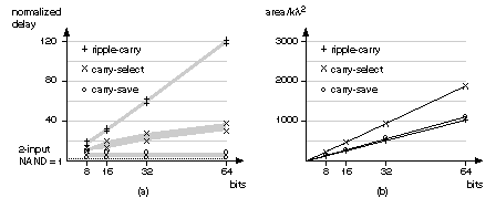
Figure 2.26 shows the normalized delay and area figures for a set of predesigned datapath adders. The data in Figure 2.26 is from a series of ASIC datapath cell libraries (Compass Passport) that may be synthesized together with test vectors and simulation models. We can combine the different adder techniques, but the adders then lose regularity and become less suited to a datapath implementation.
There are other adders that are not used in datapaths, but are occasionally useful in ASIC design. A serial adder is smaller but slower than the parallel adders we have described [Denyer and Renshaw, 1985]. The carry-completion adder is a variable delay adder and rarely used in synchronous designs [Sklansky, 1960].
Chapter start Previous page Next page