Chapter start Previous page Next page
2.6.2 Adders
We can view addition in terms of generate , G[ i ], and propagate , P[ i ], signals.
G[ i ] = A[ i ] · B[ i ] G[ i ] = A[ i ] · B[ i ](2.42)
P[ i ] = A[ i ] B[ i ] P[ i ] = A[ i ] + B[ i ](2.43)
C[ i ] = G[ i ] + P[ i ] · C[ i 1] C[ i ] = G[ i ] + P[ i ] · C[ i 1](2.44)
S[ i ] = P[ i ] C[ i 1] S[ i ] = A[ i ] B[ i ] C[ i 1](2.45)
where C[ i ] is the carry-out signal from stage i , equal to the carry in of stage ( i + 1). Thus, C[ i ] = COUT[ i ] = CIN[ i + 1]. We need to be careful because C[0] might represent either the carry in or the carry out of the LSB stage. For an adder we set the carry in to the first stage (stage zero), C[1] or CIN[0], to '0'. Some people use delete (D) or kill (K) in various ways for the complements of G[i] and P[i], but unfortunately others use C for COUT and D for CINso I avoid using any of these. Do not confuse the two different methods (both of which are used) in Eqs. 2.422.45 when forming the sum, since the propagate signal, P[ i ] , is different for each method.
Figure 2.22(a) shows a conventional RCA. The delay of an n -bit RCA is proportional to n and is limited by the propagation of the carry signal through all of the stages. We can reduce delay by using pairs of "go-faster" bubbles to change AND and OR gates to fast two-input NAND gates as shown in Figure 2.22(a). Alternatively, we can write the equations for the carry signal in two different ways:
either C[ i ] = A[ i ] · B[ i ] + P[ i ] · C[ i 1](2.46)
orn C[ i ] = (A[ i ] + B[ i ] ) · (P[ i ]' + C[ i 1]),(2.47)
where P[ i ]' = NOT(P[ i ]). Equations 2.46 and 2.47 allow us to build the carry chain from two-input NAND gates, one per cell, using different logic in even and odd stages (Figure 2.22b):
C1[ i ]' = P[ i ] · C3[ i 1] · C4[ i 1] C3[ i ]' = P[ i ] · C1[ i 1] · C2[ i 1](2.48)
C2[ i ] = A[ i ] + B[ i ] C4[ i ]' = A[ i ] · B[ i ](2.49)
C[ i ] = C1[ i ] · C2[ i ] C[ i ] = C3[ i ] ' + C4[ i ]'(2.50)
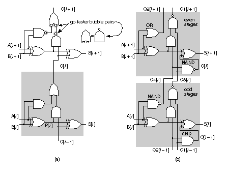
(the carry inputs to stage zero are C3[1] = C4[1] = '0'). We can use the RCA of Figure 2.22(b) in a datapath, with standard cells, or on a gate array.
Instead of propagating the carries through each stage of an RCA, Figure 2.23 shows a different approach. A carry-save adder ( CSA ) cell CSA(A1[ i ], A2[ i ], A3[ i ], CIN, S1[ i ], S2[ i ], COUT) has three outputs: