Chapter start Previous page Next page
2.10 Problems
* = Difficult,** = Very difficult, *** = Extremely difficult
2.1 (Switches, 20 min.) (a) Draw a circuit schematic for a two-way light switch: flipping the switch at the top or bottom of the stairs reverses the state of two light bulbs, one at the top and one at the bottom of the stairs. Your schematic should show and label all the cables, switches, and bulbs. (b) Repeat the problem for three switches and one light in a warehouse.
2.2 (Logic, 10 min.) The queen wished to choose her successor wisely. She blindfolded and then placed a crown on each of her three children, explaining that there were three red and two blue crowns, and they must deduce the color of their own crown. With blindfolds removed the children could see the two other crowns, but not their own. After a while Anne said: "My crown is red." How did she know?
2.3 (Minus signs, 20 min.) The channel charge in an n -channel transistor is negative. (a) Should there not be a minus sign in Eq. 2.5 to account for this? (b) If so, then where in the derivation of Section 2.1 does the minus sign disappear to arrive at Eq. 2.9 for the current in an n -channel transistor? (c) The equations for the current in a p -channel transistor (Eq. 2.15) have the opposite sign to those for an n -channel transistor. Where in the derivation in Section 2.1 does the extra minus sign arise?
FIGURE 2.34 Transistor characteristics for a 0.3 m m process (Problem 2.4). |
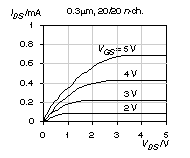
2.4 (Transistor curves, 20 min.) Figure 2.34 shows the measured I DS V DS characteristics for a 20/20 n -channel transistor in a 0.3 m m (effective gate length) process from an ASIC foundry. Derive as much information as you can from this figure.
2.5 (Body effect, 20 min). The equations for the drainsource current (2.9, 2.12, and 2.15) do not contain V SB , the source voltage with respect to the bulk, because we assumed that it was zero. This is not true for the n -channel transistor whose drain is connected to the output in a two-input NAND gate, for example. A reverse substrate bias (or back-gate bias; V SB > 0 for an n -channel transistor) makes the bulk act like a second gate (the back gate) and modifies an n -channel transistor threshold voltage as follows:
where V t 0 n is measured with V SB = 0 V; f 0 is called the surface potential; and g (gamma) is the body-effect coefficient (back-gate bias coefficient),
There are several alternative names and symbols for f 0 ("phi," a positive quantity for an n -channel transistor, typically between 0.60.7 V)you may also see f b (for bulk potential) or 2 f F (twice the Fermi potential, a negative quantity). In Eq. 2.68, e Si = e 0 e r = 1.053 ¥ 10 10 Fm 1 is the permittivity of silicon (the permittivity of a vacuum e 0 = 8.85 ¥ 10 12 Fm 1 and the relative permittivity of silicon is e r = 11.7); NA is the acceptor doping concentration in the bulk (for p -type substrate or well ND for the donor concentration in an n -type substrate or well); and C ox is the gate capacitance per unit area given by
- a. Calculate the theoretical value of g for NA = 10 16 cm 3 , Tox = 100 Å.
- b. Calculate and plot V t n for V SB ranging from 0 V to 5 V in increments of 1 V assuming values of g = 0.5 V 0.5 , f 0 = 0.6 V, and V t0 n = 0.5 V obtained from transistor characteristics.
- c. Fit a linear approximation to V t n .
- d. Recognizing V SB £ 0 V, rewrite Eq. 2.67 for a p -channel device.
- e. (Harder) What effect does the back-gate bias effect have on CMOS logic circuits?
Answer: (a) 0.17 V 0.5 (b) 0.501.3 V.
2.6 (Sizing layout, 10 min.) Stating clearly whatever assumptions you make and describing the tools and methods you use, estimate the size (in l ) of the standard cell shown in Figure 1.3. Estimate the size of each of the transistors, giving their channel lengths and widths (stating clearly which is which).
2.7 (CMOS process) (20 min.) Table 2.15 shows the major steps involved in a typical deep submicron CMOS process. There are approximately 100 major steps in the process.
- a. If each major step has a yield of 0.9, what is the overall process yield?
- b. If the process yield is 90 % (not uncommon), what is the average yield at each major step?
- c. If each of the major steps in Table 2.15 consists of an average of five other microtasks, what is the average yield of each of the 500 microtasks.
- d. Suppose, for example, an operator loads and unloads a furnace five times a day as a microtask, how many days must the operator work without making a mistake to achieve this microtask yield?
- e. Does this seem reasonable? What is wrong with our model?
- f. (**60 min.)
Draw the process cross-section showing, in particular, the poly, FOX, gate
oxide, IMOs and metal layers. You may have to make some assumptions about
the meanings and functions of the various steps and layers. Assume all
layers are deposited on top of each other according to the thicknesses
shown (do not attempt to correct for the silicon consumed during oxidationeven
if you understand what this means). The abbreviations in Table 2.15
are as follows: dep. = deposition;
LPCVD = low-pressure
chemical vapor deposition (for growing oxide and poly); LDD = lightly
doped drain (a way to improve transistor characteristics); SOG = silicon
overglass (a deposited quartz to help with step coverage between metal
layers).
TABLE 2.15 CMOS process steps (Problem 2.7). 1
Answer: (a) Zero. (b) 0.999. (c) 0.9998. (d) 3 years.
2.8 (Stipple patterns, 30 min.)
- a. Check the stipple patterns in Figure 2.9. Using ruled paper draw 8-by-8 stipple patterns for all the combinations of layers shown.
- b. Repeat part a for Figure 2.10.
2.9 (Select, 20 min.) Can you draw a design-rule correct (according to the design rules in Tables 2.72.9) layout with a piece of select that has a minimum width of 2 l (rule 4.4)?
2.10 (*Inverter layout, 60 min.) Using 1/4-inch ruled paper (or similar) draw a minimum-size inverter (W/L = 1 for both p -channel and n -channel transistors). Use a scale of one square to 2 l and the design rules in Table 2.7Table 2.9. Do not use m2 or m3only m1. Draw the nwell, pwell, ndiff, and pdiff layers, but not the implant layers or the active layer. Include connections to the input, output, VDD, and VSS in m1. There must be at least one well connection to each well ( n -well to VDD, and p -well to VSS). Minimize the size of your cell BB. Draw the BB outline and write its size in l 2 on your drawing. Use green diagonal stripes for ndiff, brown diagonal stripes for pdiff, red diagonal stripes for poly, blue diagonal stripes for m1, solid black for contact). Include a key on your drawing, and clearly label the input, output, VDD, and VSS contacts.
2.11 (*AOI221 Layout, 120 min.) Layout the AOI221 shown in Figure 2.13 with the design rules of Tables 2.72.9 and using Figure 1.3 as a guide. Label clearly the m1 corresponding to the inputs, output, VDD bus, and GND (VSS) bus. Remember to include substrate contacts. What is the size of your BB in l 2 ?
- a. Using the values for sheet resistance shown in Table 2.3, calculate the resistance of a 200 l long (in the direction of current flow) by 3 l wide piece of each of the layers.
- b. Estimate the resistance of an 8-inch, 10 W cm, p -type, <100> wafer, measured (i) from edge to edge across a diameter and (ii) from face center to the face center on the other side.
2.13 (*Layout graphics, 120 min.) Write a tutorial for capturing layout. As an example:
To capture EPSF (encapsulated PostScript format) from Tanner Research's L-Edit for documentation, Macintosh version... Create a black-and-white technology file, use Setup, Layers..., in L-Edit. The method described here does not work well for grayscale or color. Use File, Print..., Destination check button File to print from L-Edit to an EPS (encapsulated PostScript) file. After you choose Save, a dialog box appears. Select Format: EPS Enhanced Mac Preview, ASCII, Level 1 Compatible, Font Inclusion: None. Save the file. Switch to Frame. Create an Anchored Frame. Use File, Import, File... to bring up a dialog box. Check button Copy into Document, select Format: EPSF. Import the EPS file that will appear as a "page image". Grab the graphic inside the Anchored Frame and move the "page image" around. There will be a footer with text on the "page image" that you may want to hide by using the Anchored Frame edges to crop the image.
Your instructions should be precise, concise, assume nothing, and use the names of menu items, buttons and so on exactly as they appear to the user. Most of the layout figures in this book were created using L-Edit running on a Macintosh, with labels added in FrameMaker. Most of the layouts use the Compass layout editor.
2.14 (Transistor
resistance, 20 min.)
Calculate I
DS and the resistance (the DC value
V DS /
I DS as well as the AC value
![]() as appropriate) of long-channel transistors with the following parameters,
under the specified conditions. In each case state whether the transistor
is in the saturation region, linear region, or off:
as appropriate) of long-channel transistors with the following parameters,
under the specified conditions. In each case state whether the transistor
is in the saturation region, linear region, or off:
(i) n -channel: V t n = 0.5 V, b n = 40 m AV 2 :
V GS = 3.3V: a. V DS = 3.3 V b. V DS = 0.0 V c. V GS = 0.0 V, V DS = 3.3 V
(ii) p -channel: V t p = 0.6 V, b p = 20 m AV 2 :
V GS = 0.0 V: a. V DS = 0.0 V b. V DS = 5.0 V c. V GS = 5.0 V, V DS = 5.0 V
2.15 (Circuit theory, 15 min.) You accidentally created the "inverter" shown in Figure 2.35 on a full-custom ASIC currently being fabricated. Will it work? Your manager wants a yes or no answer. Your group is a little more understanding: You are to make a presentation to them to explain the problems ahead. Prepare two foils as well as a one page list of alternatives and recommendations.
FIGURE 2.35 A CMOS "inverter" with n-channel and p-channel transistors swapped (Problem 2.15). |
|

2.16 (Mask resolution, 10 min.) People use LaserWriters to make printed-circuit boards all the time.
- a. Do you think it is possible to make an IC mask using a 600 dpi (dots per inch) LaserWriter and a transparency?
- b. What would l be?
- c. (Harder) See if you can use a microscope to look at the dot and the rectangular bars (serifs) of a letter 'i' from the output of a LaserWriter on paper (most are 300 dpi or 600 dpi). Estimate l . What is causing the problem? Why is there no rush to generate 1200 dpi LaserWriters for paper? Put a page of this textbook under the microscope: can you see the difference? What are the similar problems printing patterns on a wafer?
2.17 (Lambda, 10 min.) Estimate l
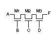
2.18 (Pass-transistor logic, 10 min.)
- a. In Figure 2.36 suppose we set A = B = C = D = '1', what is the value of F?
- b. What is the logic strength of the signal at F?
- c. If V DD = 5 V and V t n = 0.6 V, what would the voltage at the source and drain terminals of M1, M2, and M3 be?
- d. Will this circuit still work if V DD = 3 V?
- e. At what point does it stop working?
2.19 (Transistor
parameters, 20 min.)
Calculate the (a) electron and (b) hole mobility
for the transistor parameters given in Section 2.1 if ![]() = 80
mA V 2 and
= 80
mA V 2 and ![]() = 40
mA V 2 .
= 40
mA V 2 .
Answer: (a) 0.023 m 2 V 1 s 1 .
2.20 (Quantum behavior, 10 min.) The average thermal energy of an electron is approximately k T, where k = 1.38 ¥ 10 23 JK 1 is Boltzmann's constant and T is the absolute temperature in kelvin.
- a. The kinetic energy of an electron is (1/2) m v 2 , where v is due to random thermal motion, and m = 9.11 ¥ 10 31 kg is the rest mass. What is v at 300 K?
- b. The electron wavelength l = h / p , where h = 6.62 ¥ 1034 Js is the Planck constant, and p = m v is the electron momentum. What is l at 25 C?
- c. Compare the thermal velocity with the saturation velocity.
- d. Compare the electron wavelength with the MOS channel length and with the gate-oxide thickness in a 0.25 m m process and a 0.1 m m process.
2.21 (Gallium arsenide, 5 min.) The electron mobility in GaAs is about 8500 cm 2 V 1 s 1 ; the hole mobility is about 400 cm 2 V 1 s 1 . If we could make complementary n -channel and p -channel GaAs transistors (the same way that we do in a CMOS process) what would the ratio of a GaAs inverter be to equalize rise and fall times? About how much faster would you expect GaAs transistors to be than silicon for the same transistor sizes?
2.22 (Margaret of Anjou, 5 min.)
- a. Why is it ones' complement but two's complement?
- b. Why Queen's University, Belfast but Queens' College, Cambridge?
2.23 (Logic cell equations, 5 min.) Show that Eq. 2.31, 2.36, and 2.37 are correct.
2.24 (Carry-lookahead equations, 10 min.)
- a. Derive the carry-lookahead equations for i = 8. Write them in the same form as Eq. 2.56.
- b. Derive the equations for the BrentKung structure for i = 8.
2.25 (OAI cells, 20 min.) Draw a circuit schematic, including transistor sizes, for (a) an OAI321 cell, (b) an AOI321 cell. (c) Which do you think will be larger?
2.26 (**Making stipple patterns) Construct a set of black-and-white, transparent, 8-by-8 stipple patterns for a CMOS process in which we draw both well layers, the active layer, poly, and both diffusion implant layers separately. Consider only the layers up to m1 (but include m1 and the contact layer). One useful tool is the Apple Macintosh Control Panel, 'General Controls,' that changes the Mac desktop pattern.
- a. (60 min.) Create a set of patterns with which you can detect any errors (for example, n -well and p -well overlap, or n -implant and p -implant overlap).
- b. (60 min.+) Using a layout of an inverter as an example, find a set of patterns that allows you to trace transistors and connections (a very qualitative goal).
- c. (Days+) Find a set of grayscale stipple patterns that allow you to produce layouts that "look nice" in a report (much, much harder than it sounds).
2.27 (AOI and OAI cells, 10 min.). Draw the circuit schematics for an AOI22 and an OAI22 cell. Clearly label each transistor as on or off for each cell for an input vector of (A1, A2, B1, B2) = (0101).
2.28 (Flip-flops and latches, 10 min.) In no more than 20 words describe the difference between a flip-flop and a latch.
2.29 (**An old argument) Should setup and hold times appear under maximum, minimum, or typical in a data sheet? (From Peter Alfke.)
2.30 (***Setup, 20 min.) "There is no such thing as a setup and hold time, just two setup timesfor a '1' and for a '0'." Comment. (From Clemenz Portmann.)
2.31 (Subtracter, 20 min.) Show that you can rewrite the equations for a full subtracter (Eqs. 2.652.66) to be the same as a full adderexcept that A is inverted in the borrow out equation, as follows:
DIFF = A B BIN = SUM(A, B, BIN)(2.70)
BOUT = NOT(A) · B + NOT(A) · BIN + B · BIN = MAJ(NOT(A), B, CIN)(2.71)
Explain very carefully why we need to connect BIN[0] to VSS. Show that for a subtracter implemented by inverting the B input of an adder and setting CIN[0] = '1', the true overflow for ones' complement or two's complement representations is XOR(CIN[MSB], CIN[MSB 1]). Does this hold for the above subtracter?
2.32 (Complex CMOS cells) Logic synthesis has completely changed the nature of combinational logic design. Synthesis tools like to see a huge selection of cells from which to choose in order to optimize speed or area.
- a. (20 min.) How many AOI nnnn cells are there, if the maximum value of n = 4?
- b. (30 min.) Consider cells of the form AOI nnnn where n can be negativeindicating a set of inputs are inverted. Thus, an AOI-22 (where the hyphen '-' indicates the following input is inverted) is a NOR(NOR(A, B), AND(C, D)), for example. How many logically different cells of the AOI xxxx family are there if x can be '-2', '-1', '1', or '2' with no more than four inputs? Remember the AOI family includes OAI, AO, and OA cells as well as just AOI. List them using an extension to the notation for a cell with mixed-sign inputs: for example, an AO(1-1)1 cell is NOT(NOR(AND(A, NOT(B)), C)). Hint: Be very careful because some cells with negative inputs are logically equivalent to others with positive inputs.
- c. (10 min.) If we include NAND and NOR cells with inverting inputs in a library, how many different cells in the NAND family are there with four or fewer inputs (the NAND family includes NOR, AND, and OR cells)?
- d. (30 min.) How many cells in the AOI and NAND families are there with four inputs or less that use fewer than eight transistors? Include cells that are logically equivalent but have different physical implementations. For example, a NAND1-1 cell, requiring six transistors, is logically equivalent to an OR1-1 cell that requires eight transistors. The OR1-1 implementation may be useful because the output inverter can easily be sized to produce an OR1-1 cell with higher drive.
- e. (**60 min.) How many cells are there with fewer than four inputs that do not fit into the AOI or NAND families? Hint: There is an inverter, a buffer, a half-adder, and the three-input majority function, for example.
- f. (***) Recommend a better, user-friendly, naming system (which is also CAD tool compatible) for combinational cells.
2.33 (**Design rules, 60 min.) A typical set of deep submicron CMOS design rules is shown in Table 2.16. Design rules are often confusing and use the following "buzz-words," perhaps to prevent others from understanding them.
- The end cap is the extension of poly gate beyond the active or diffusion.
- Overlap . Normally one material is completely contained within the other, overlap is then the amount of the "surround."
- Extension refers to the extension of diffusion beyond the poly gate.
- Same (in a spacing rule) means the space to the same type of diffusion or implant.
- Opposite refers to the space to the opposite type of diffusion or implant.
- A dogbone is the area surrounding a contact. Often the spacing to a dogbone contact is allowed be slightly less than to an isolated line.
- Field is the area outside the active regions. The field oxide (sandwiched between the diffusion layers and the poly or m1 layers) is thicker than the gate oxide and separates transistors.
- Exact refers to contacts that are all the same size to simplify fabrication.
- A butting contact consists of two adjacent diffusions of the opposite type (connected with metal). This occurs when a well contact is placed next to a source contact.
- Fat metal . Some design rules use different spacing for metal lines that are wider than a certain amount.
- a. Draw a copy of the MOSIS rules as shown in Figure 2.11, but using the rule numbers and values in microns and l from Table 2.16.
- b. How compatible are the two sets
of rules?
TABLE 2.16 ASIC design rules (Problem 2.33). Absolute values in microns are given for l = 0.2 m m.
Rule 2
- a. Explain carefully why a CMOS device can withstand a 2000 V ESD event when the gate breakdown voltage is only 510 V, but that shorting a device pin to a 10 V supply can destroy it.
- b. Explain why an electric shock from a 240 VAC supply can kill you, but an 3000 VDC shock from a static charge (walking across a nylon carpet and touching a metal doorknob) only gives you a surprise.
2.35 (*Stacks in CMOS cells, 60 min.)
- a. Given a CMOS cell of the form AOI ijk or OAI ijk ( i, j, k > 0) derive an equation for the height (the number of transistors in series) and the width (the number of transistor in parallel) of the n -channel and p -channel stacks.
- b. Suppose we increase the number of indices to four, i.e. AOI ijkl . How do your equations change?
- c. If the stack height cannot be greater than three, which three-index AOI ijk and OAI ijk cells are illegal? Often limiting the stack height to three or four is a design rule for radiation-hard librariesuseful for satellites.
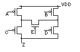
2.36 (Duals, 20 min.) Draw the n -channel stack (including device sizes, assuming a ratio of 2) that complements the p -channel stack shown in Figure 2.37.
FIGURE 2.37 A p -channel stack using a bridge device, E (Problem 2.36). |
2.37 (***FPGA conditional-sum adder, days+) A Xilinx application-note (M. Klein, "Conditional sum adder adds 16 bits in 33 ns," Xilinx Application Brief, Xilinx data book, 1992, p. 6-26) describes a 16-bit conditional-sum adder using 41 CLBs in three stages of addition; see also [Sklansky, 1960]. A Xilinx XC3000 or XC4000 CLB can perform any logic function of five variables, or two functions of (the same) four variables. Can you find a solution with fewer CLBs in three stages? Hint: R. P. Halverson of the University of Hawaii produced a solution with 36 CLBs.
2.38 (Encoding, 10 min.) Booth's algorithm was suggested by a shortcut used by operators of decimal calculating machines that required turning a handle. To multiply 5 by 23 you set the levers to 5 and turned the handle three times, change gears and turn twice more.
- a. Show how to convert 1010111 (decimal
87) to the CSD vector
 .
.
- b. Convert 1000101 to the CSD vector.
- c. How do you know that
 (decimal 101)
is not the CSD vector representation of 1100101 (decimal 101)?
(decimal 101)
is not the CSD vector representation of 1100101 (decimal 101)?
1. Depths of layers are in angstroms (negative values are etch depths). For abbreviations used, see Problem 2.7.
2. sp. = space; ov. = overlap; same = same diffusion or implant type; opposite = opposite implant or diffusion type;
diff = p+ or n+; p+ = p+ diffusion; n+ = n+ diffusion; implant = p+ or n+ implant select.
Chapter start Previous page Next page